Hard Disk vs SSDs
A Hard disk drive reads data with a mechanical arm on a spinning plater, here the sequential operations work well, but for random access these mechanical parts need to seek the address to be operated on, that constraint this to just 150-200 IPOS(random IO operations)/sec.
But SSDs have no moving parts, no delays, so it can easily achieve 500k IOPS/sec or even more
Q But how SSD is that fast ?
A
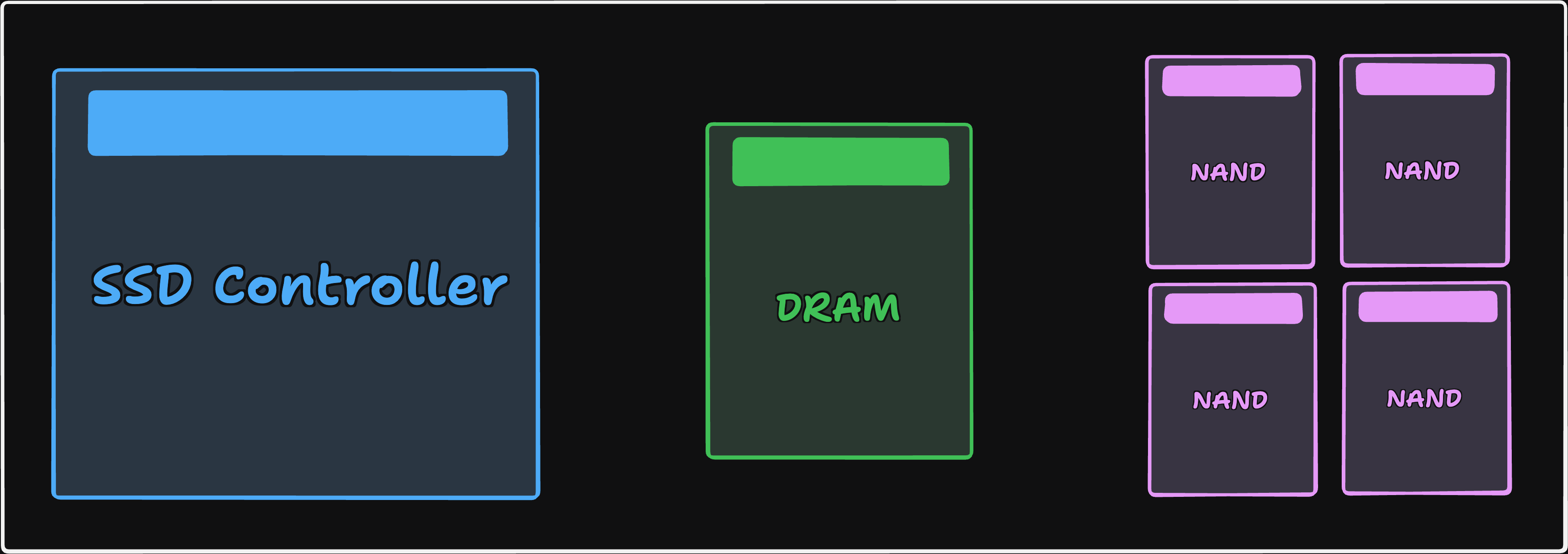 For that we need to understand the Internal architecture of SSDs, there are three main components of SSDs
- Controller - Small CPU that runs the drives firmware, it’s built in software, it manages how to store, where to write, how to optimize writes etc..
- DRAM(Dynamic Random Access memory) cache - fast, volatile memory used as computer’s main RAM, a small amount of it is usually sits on the SSD to hold the mapping table, some SSDs will skip this RAM part and use the computers own RAM instead, but majority of them have
- NAND flash chips - It’s an electronic circuit with convenient properties for retaining state. There are multiple of them present in an SSD. Each chip is called a die. These die’s are the actual storage it means the grids of tiny transistors that trap electrical charge to store your bits
At a given time the controller writes the data to many die’s in parallel and that’s why we can achieve much high throughput
Q How does each cell in the NAND stores the data ?
A 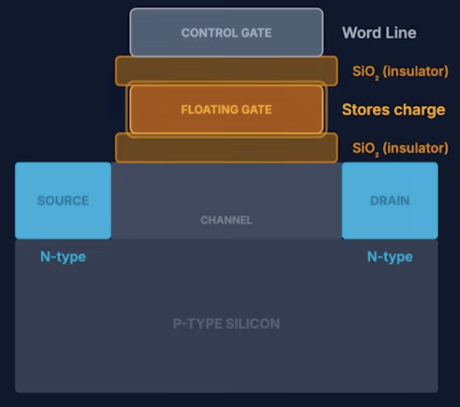
- Each memory cell is a special type of transistor called a floating-gate transistor, which acts like a tiny electronic switch controlling the flow of electrons.
- Inside this transistor, there is a floating gate, a small conductive layer completely surrounded by an insulating material (usually silicon dioxide). Because it is fully insulated, it has no direct electrical connection, which is why it is called floating
- To understand how data is stored, we need to know three parts:
- Source - where electrons enter the transistor
- Drain - where electrons exit
- Channel - the path electrons travel through from source to drain
- To store data, a high voltage (around 15–20V) is applied to the control gate
- This creates a strong electric field that forces electrons to tunnel through the insulating layer and get trapped inside the floating gate
- Even after removing the voltage, these electrons remain trapped due to the insulation
- So that’s why NAND can store data even without electricity
- This process of Trapping electrons to store, sensing them to read and Release them to erase is called Charge trap
- This single floating gate is an legacy design, nowadays we stack many floating gate layers, and they work in parallel
Q How to cells are organized in NAND storage ?
A
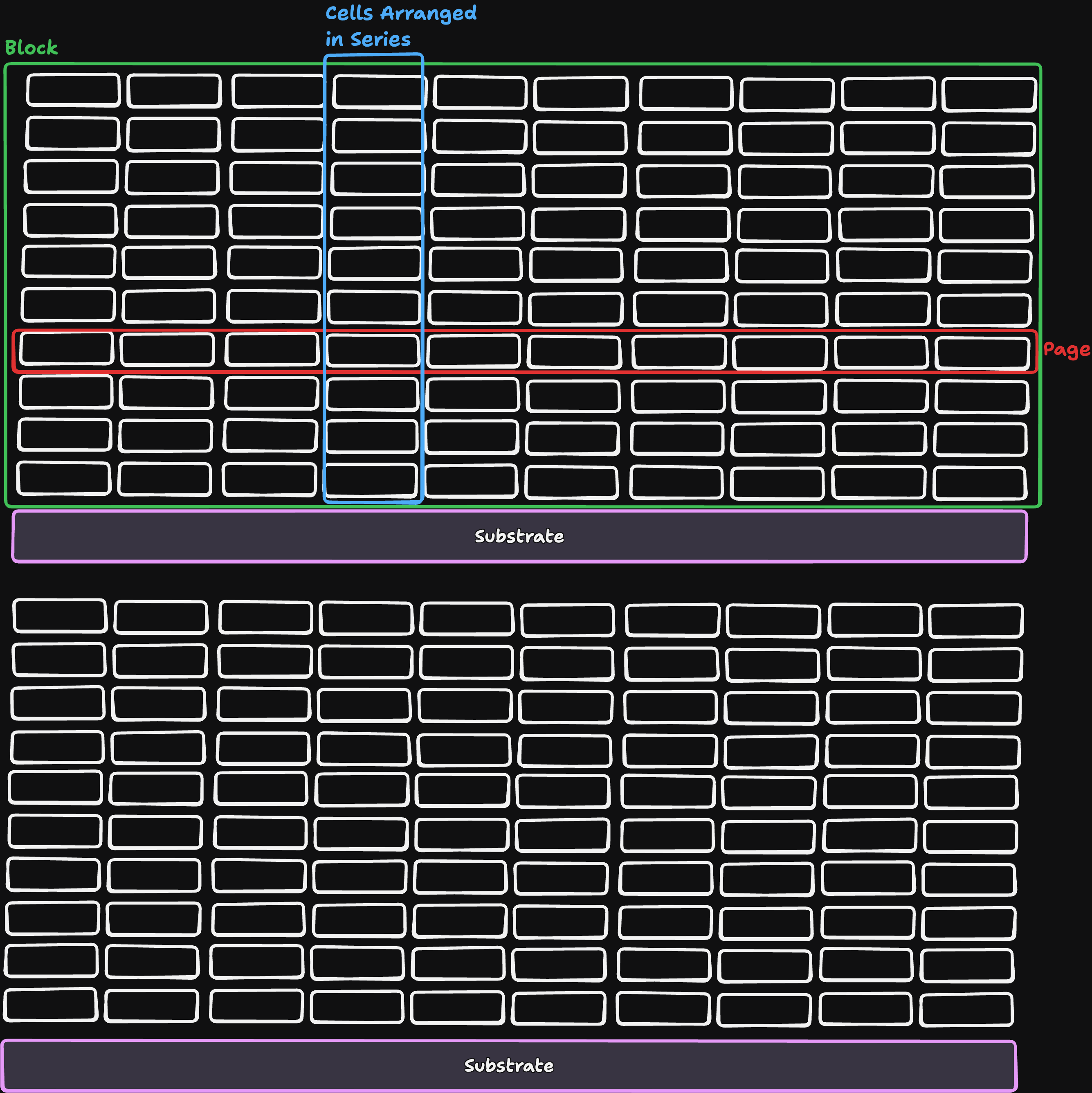
- These cells are connected in series (which is why it is called NAND storage, inspired by a NAND logic gate). There is also an alternative called NOR storage, where cells are connected in parallel
- Since the cells are in series, current has to pass through every cell in that chain to read data.
- All these cells are organized in a structured format:
- Multiple series-connected cells form a string
- Multiple strings placed side-by-side form a page (this is not the same as an OS memory page)
- A group of pages forms a block
- If we know the size of a page, we can estimate how many cells are connected in a string. Typically, this is around 128 or 256 cells per string
- Each block has its own substrate, which leads to some important constraints:
- We cannot modify a single value directly inside a page
- To update data, we must erase the entire block first, as the data is scattered around floating gates of multiple cells
- Operation rules:
- Read - we can read any page independently
- Write - must be done sequentially (in order)
- Overwrite/Update - not possible without erasing the block
Q The write and read are manageable, but how do we work around with updating the data without erasing the whole block ?
A 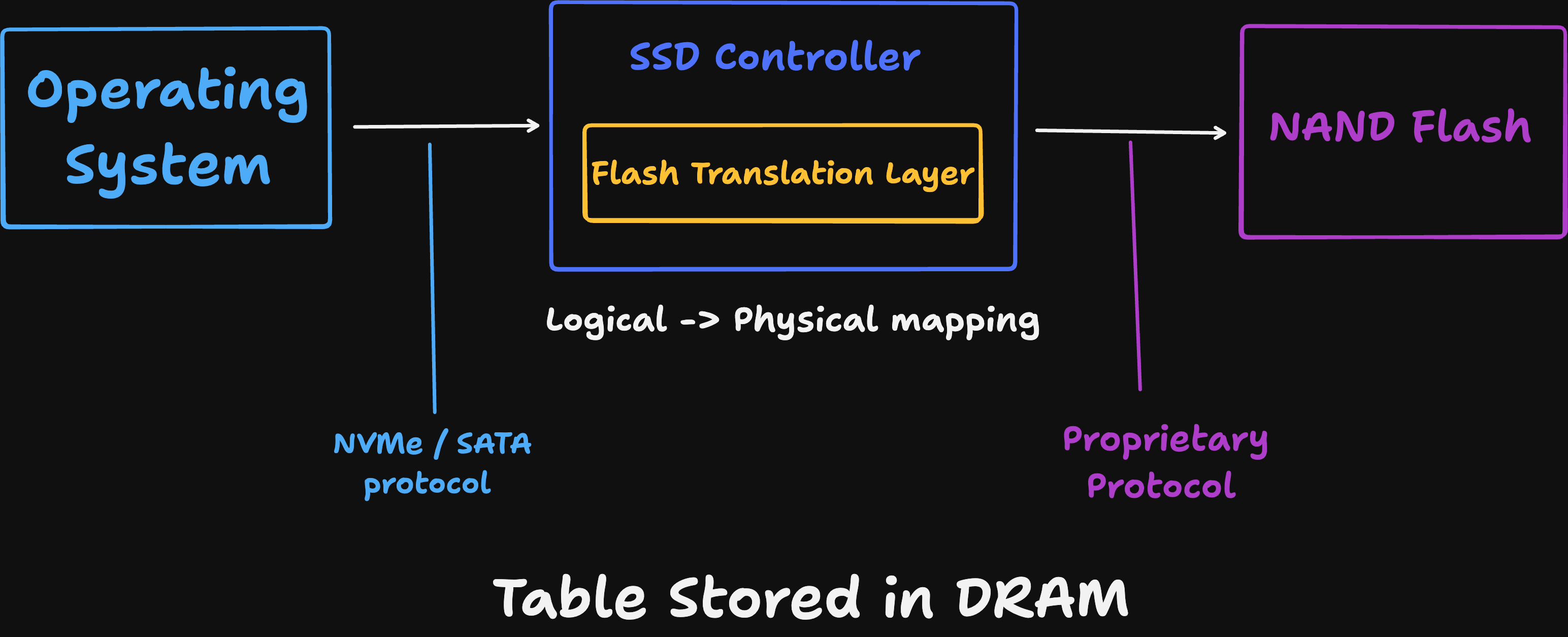
- Thus, we use the Flash Translation Layer (FTL). The OS does not write directly to NAND flash instead, all requests go through the SSD controller, which manages how data is stored internally
- The SSD controller keeps track of all data using an FTL mapping table, which maps logical addresses (from the OS) to physical locations in NAND
- Now, to update a value, we do not overwrite it in place. Instead, we:
- write a new copy of the data to a different location
- update the mapping table to point to this new location
- the old data becomes stale (invalid) since nothing references it anymore
- After some time, garbage collection (GC) kicks in. It selects blocks with a mix of valid and stale data and reclaims space in three steps:
- copy → move valid data to a new block
- clean (erase) → erase the old block
- update mapping table → update references to new locations
- This means we are doing multiple physical writes for a single logical write, which is called write amplification
- on a fresh drive, write amplification is close to ~1
- on a full or fragmented drive, it can go up to ~5–10+ (depends on workload and controller)
- This garbage collection process happens repeatedly, and NAND flash can only handle a limited number of program/erase (P/E) cycles because the oxide layer degrades over time. Consumer SSDs typically support ~1000–3000 cycles (correct for TLC NAND, higher for MLC, lower for QLC)
- To reduce uneven wear, SSDs use wear leveling:
- the controller distributes writes evenly across blocks
- it may move cold data (rarely changed data) to less-used blocks to ensure all blocks age uniformly
- Since this layer is separate from the OS, when a file is deleted in the OS, the NAND flash does not automatically know that the data is no longer needed
- To solve this, the OS sends a TRIM command, which tells the SSD which data is no longer valid
- during the next garbage collection, this data is not copied, making GC more efficient and reducing write amplification
Q Why we can only store one value(0 or 1) on the cell ?
A A NAND flash cell stores data as electrical charge in the floating gate, and originally it was designed to represent only two states: charge or no charge. This corresponds to binary values 0 and 1, and this type is called SLC (Single-Level Cell), where each cell stores exactly one bit
- However, modern NAND can store more than one bit per cell by using multiple distinct charge levels instead of just two. The controller does not simply check whether charge exists; it measures how much charge is stored and maps that to a specific binary value
- The correct relationship between charge levels and bits is as follows: two charge levels store one bit (SLC), four charge levels store two bits (MLC), eight charge levels store three bits (TLC), and sixteen charge levels store four bits (QLC). For example, in SLC, a low charge might represent 1 and a high charge represents 0. In MLC, four charge levels can represent combinations like 00, 01, 10, and 11. In TLC, eight charge levels represent values from 000 to 111, and in QLC, sixteen levels represent values from 0000 to 1111. As we increase the number of bits per cell, the charge levels become closer together, which makes it harder to distinguish between them accurately
- Because of this, higher-density cells like TLC and QLC are more error-prone, require more precise sensing, and have slower read and write speeds compared to SLC. They also have a shorter lifespan because repeated program/erase cycles degrade the insulating oxide layer, and tighter charge margins increase wear sensitivity. Additionally, storing more bits per cell increases internal work such as error correction and garbage collection. Despite these drawbacks, TLC and QLC are widely used because they allow significantly higher storage density on the same silicon, making SSDs much cheaper per gigabyte
- as 0 and 1 resembles charge, we can only store 0 or 1, but there is a way to store more than one value, we can store 4 values depicting 2 different levels of charge, 8 levels can store 3 bits, 4 levels can store 16 bits, but as these increase the complexity increases, more error prone as charge levels get closer, reads are slower and cells life would be less, as there will be huge amount of data Garbage collector needs to process, all this extra storage will happen on the same silicon
Best Practices for SSDs:
- Don’t overfill the drive, keep 7–28% of the capacity free so garbage collection has room to operate
- As the drive gets full, write amplification increases, which in turn increases latency
- To maintain steady performance, monitor the drive after regular intervals of usage (e.g., every few months)
- Use
smartctl -a disk0regularly and monitor the “Percentage Used” metric