- The registers are present in the Microprocessor of the Computer System
- The Registers are made of set of flip-flops, An 8 bit register is made of 8 flip-flops
- These are General Purpose Registers, given to the programmer to use in programs
- In 8085 there are seven, 8 bit registers (Accumulator, B, C, D, E, H, L)
- Other than these all other are special purpose registers
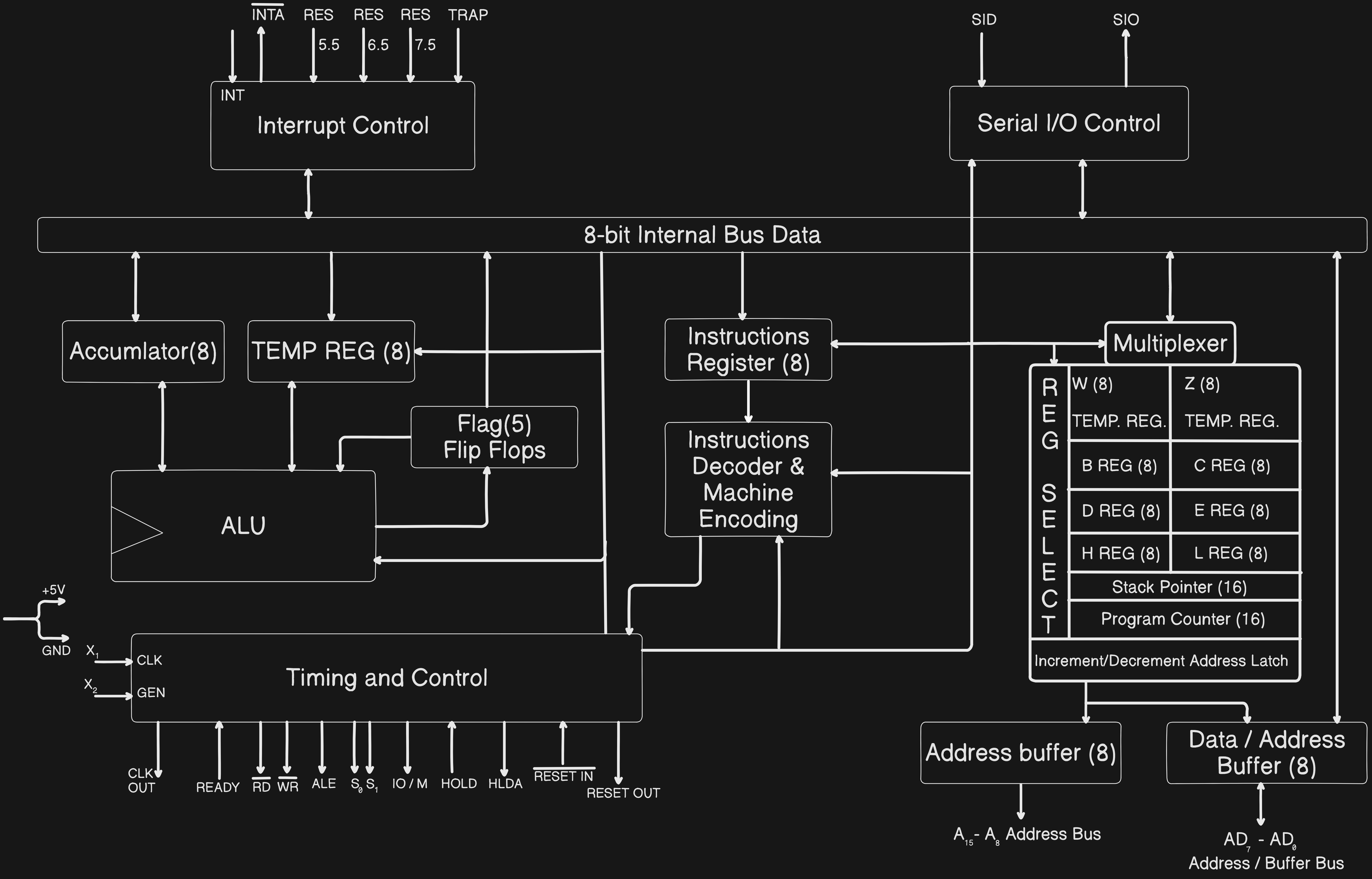
- The Program Execution Start from PC (Program Counter) which brings the first address of the program to be executed from Memory via Data bus and incremented by the Increment/Decrement Address latch and get whole program
- Then the 16-bit address will split into 8-bit and 8-bit and go into Address buffer and Data/Address Buffer and get the
Intructionsvia data bus from memory and then that data will go to 8-bit Internal Bus and the Instructions will get stored in Instructions Register and then it will get Decoded by Instruction Decoder & Machine Encoding and Timing and Control get it and broadcast control signals to the whole architecture and tell them what to do - In two inputs that go in ALU one will be definitely go from
A-Accumlator. In general mathematics we write asA = B + C, where Addition of B and C will be stored in A. But in assembly we write asADD Bhere the addition of A (pre-defined no need to specify) and B will be stored in A - In architecture, to add two numbers, First number data will be in
A Register (Accumlator Register)and theTiming and Control Circuitwill Take the value from the other corresponding Register from REG SELECT (Register Select) and move them toALUand perform the Operation and store them in theA Register (Accumlator Register). When this Operations will be going on then, In betweenProgram Counterwill be incrementing and storing the next set of Instructions in the memory - The Flag Register stores the status(not value) of the
current resultof the operations done by ALU. For example, if we want to compare two numbers, we subtract them, here if the answer is positive then A > B, if negative A < B, if zero A = B. here we don’t care about the result, we only care about the status of the result and this is what flags store - And if there is an Carry in the Addition
ALUwill togglecarry flagand read it for next set of additions, that’s the reason of two-way communication of theALUandFlag Register - And we can use the registers of same row as pairs like we can use
BandCRegisters as Pairs, but notBandDRegisters, when use them as pairs the order of values will be taken with respect to Little Indian Rule. - And the
WandZare temporary register pair, they are not accessible to the programmer, not even to read, they are used by CPU for some specific operations - In Memory there will be
Programs,Data(with their corresponding Address) andStacks. The Difference isStacksstore in structured form andDatastore in Unstructured form.
Q Why don’t we use Queue in place of Stack ?
A If we use Queue we need to handle 2 addresses, one of the first element and another of last element, but in stack we don’t need to track the address of first element
- The Stack pointer Stores the Address of the Last Element(Top Element) of the Stack. The stacks are used at the places where we want to store the data in the structured format. For example, The gallery of our phone uses stack as it shows the recent images and go on to the older images
- When we
PushStack pointer will be decremented(as will move to higher address) and when wePopStack pointer decrements, This incrementing and decrementing of bothStack PointerandProgram Counteris done byIncrement/Decrement Address Latch
8085 Pin Diagram
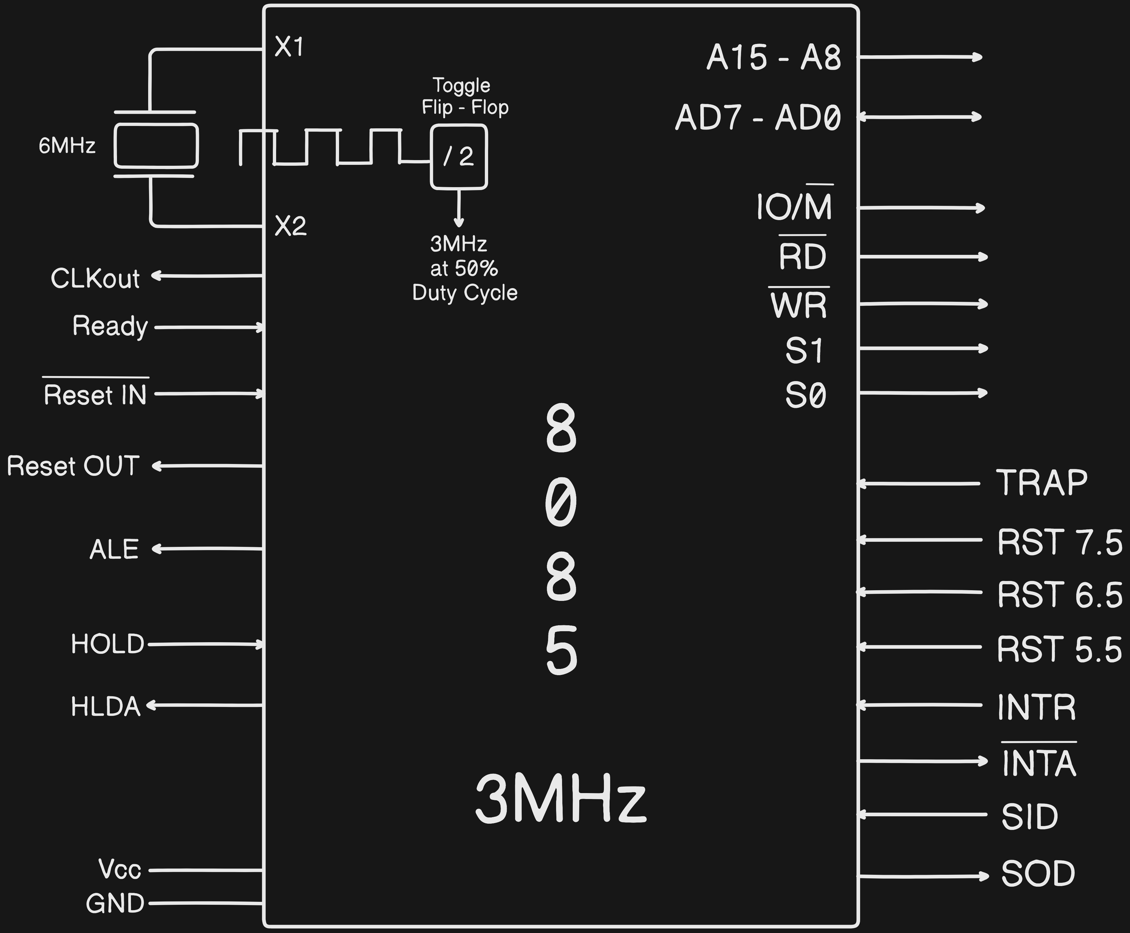
- The X1 and X2 will provide Clock to the Toggle Flip-Flop which converts it’s frequency to
3MHzand give to Microprocessor
Q But if we need to provide 3MHz why we are using clock of 6MHz ?
A The clocks will not be exactly 3MHz frequency they will have error, thus we take Crystal of 6MHz and half it to 3MHz with Toggle Flip Flop
- The CLKout is used to send out the
clockto other devices - The Microprocessor are fast, when are transferring the data to other devices like pen drive they cannot keep up with Microprocessor Speed so, the Ready Pin is used to control the speed of the data sent, if Ready State is
1we will send data, if0will keep checking when it’s1 - The Reset IN is used to reset the microprocessor, It has bar on it which says it’s active at
0and unactive at1. After thisReset INwill send reset signal to Reset OUT which broadcast signal to whole computer system to reset, if they require reset they will reset - To Understand ALE (Address Latch Enable) we need to understand Multiplexing
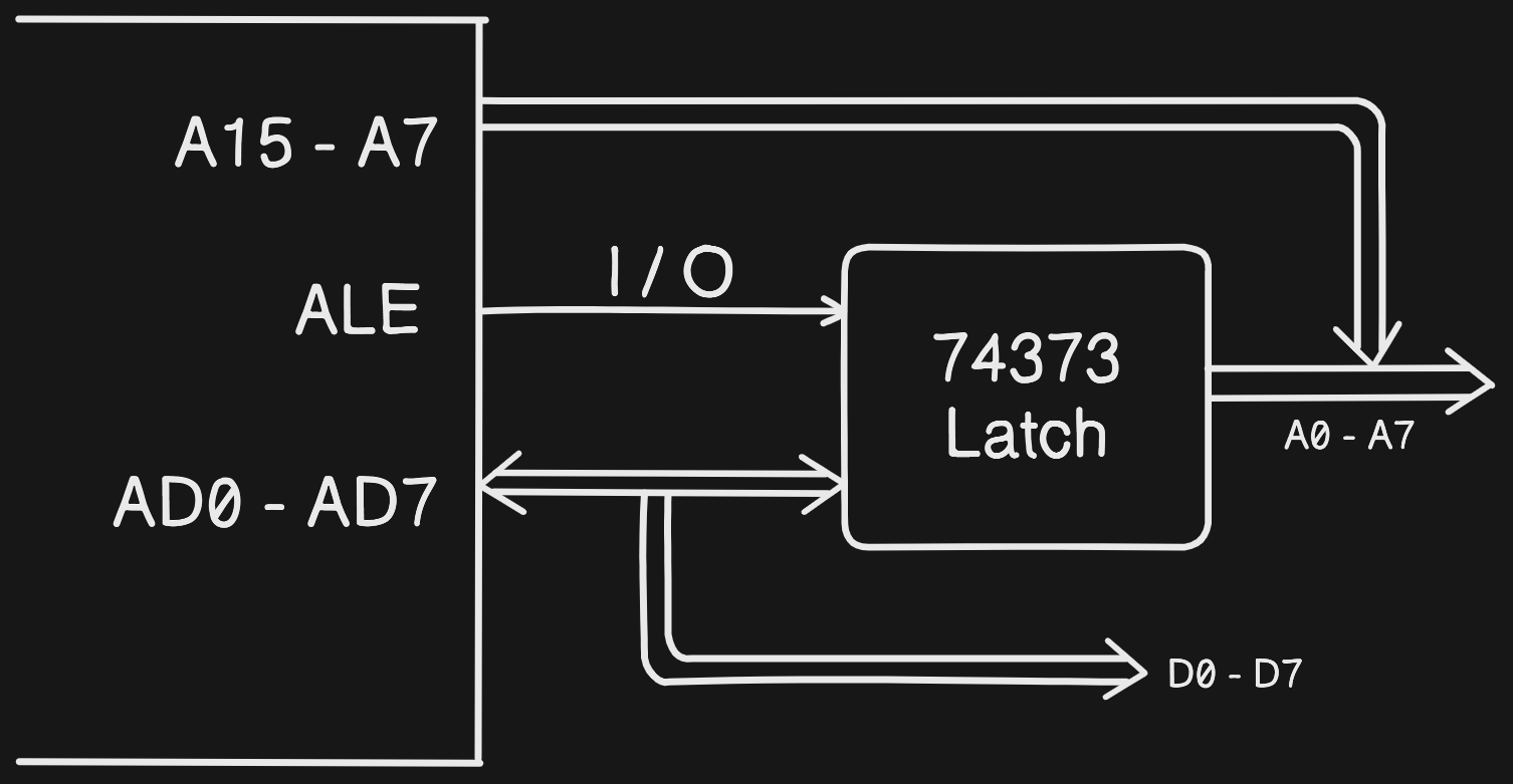
- In the above image the
A15 - A7are used as Address, butAD0 - AD7are club ofA0 - A7andD0 - D7which can be used to pass both Address and Data, IfALE = 1thenAD0 - AD7have Address, ifALE = 0thenAD0 - AD7have data - The three pins IO/M, RD, WR are as same as discussed in this table. To understand it we use below Image In which we give Inputs to the
Multiplexerand it perform subsequent operations and theXin the diagram represents that operations doesn’t exist 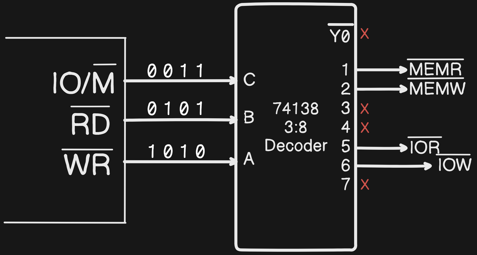
- S1 and S0 are Status Signals,
S1is taken as1when Microprocessor gives Output,S0is1when Microprocessor Reads the Data. - SID(Serial Input Data) and SOD(Serial Output Data) are used for serial communication. for context the A15 - A7 and AD7 - AD0 are used for parallel Communication
- The TRAP, RST 7.5, RST 6.5, RST 5.5, INTR are interrupts; these are provided to the microprocessors when they’re running the program. Later, it will be passed on to the Interrupt Service Routine, and it will solve the problem of the interrupt, allowing the microprocessor to continue executing the program.
Q What happens when multiple interrupts come at a time to the Microprocessor ?
A We consider the Interrupts via Priority, the priority Order is same as the Pins in the Microprocessor. TRAP, RST 7.5, RST 6.5, RST 5.5, INTR
- The INTA will send the Interrupt response of the INTR
- The HOLD and HLDA is used in DMA(Direct Memory Access). If we want to transfer data from
MemorytoI/Othen we transfer it viaMicroproceesor, It’s good but when we want to transfer a lot of data we useDMAwhich means we transfer directly fromMemorytoI/Oby removingMicroproceesorin between. For this we use DMAC(DMA Controller) chip which gives HOLD command toMicroproccesorwhich holds the buses and send HLDA(HOLD Acknowledgement) signal to theDCMAand the data will be directly transferred betweenMemoryandI/Oby skippingMicroproccesorin between
Flag Register
- Flag Register will give the status of the current result, sometimes status of the
Accumlatoralso but not always 
- The X’s Present in the Diagram are don’t care Flags, which are empty and kept for future use
- CF (carry Flag) stores the carry value of the operation performed
- PF (parity Flag) tells us the number of
1'sin the result, If even number of1'sthe parity Flag will be1, If odd number of1'sthe parity Flag will be0 - AC (Auxiliary Carry) is the carry which went to
Lower nibblecarry toHigher nibblecarry. The input is divided into half and the Left half is calledHigher nibbleand the right half is calledLower nibble - ZF (Zero Flag) is
1when the result isequal to zeroand0whennot result is equal to zero - SF (Sign Flag) it tells the sign of the answer as we can’t represent the sign in the binary, so we us this flag.
SF = 1when result is-veit meansMSB(Most Significant Bit)is1andSF = 0when result is+veit meansMSB(Most Significant Bit)is0
Q What is difference between Unsigned and Signed Numbers ?
A Given an 8-bit number the Unsigned numbers range will be from 0 to 255, but in Signed numbers the range will be -128 to +128, thus unsigned number we can store more values in the same space given that our application only uses positive numbers
Q What is the value of 1000 0011 ?
A It’s not -3 It’s -7DH. Because negative values are stored in 2's Compliment
Note: The negative numbers are stored in 2's Compliment because in 2's Compliment it’s Impossible to generate negetive zero. For example, this 1000 0000 will result in - 0 which is not possible, that’s why we store negative numbers in 2's Compliment
For reference, 2's Compliment of 0000 is 0000
8085 Addressing Modes
Addressing modes is an manner in which the Operands are given to an instruction
Immediate Addressing Mode- Data is given in the Instruction. e.g.:MVI B,25H. Here in this program we directly given Address(Here 25H is Address not data, as we haveIin MVI) so there is no need to Microprocessor to go into the Memory thus this program runs very fast, thus it is called as Immediate Addressing ModeRegister Addressing Mode- Data is given in Register. e.g.:MOV B, C. Here in this we give data to the register. the value goes in B depends on theIntialised value of C. This perform same operation ofMV1 B, 25Hbut with less memoryDirect Addressing Mode- Address is given in the Instruction (not data, It is used in problems likeAdd contents of location 2000H and 3000H). e.g.:LDA 2000H. Here in thisAregister will get contents of location2000HIndirect Addressing Mode- Address is given in the Register e.g.:LDAX B, A. Here in thisA will *not* get the contents of BC Pair, It gets the Memory location pointing the contents of BC Pair, It’s BC pair not BC because it isLoad Xand BC pair is not fitted in A as it’s 16 bit and A is of 8 bits. we can do the same operation by using direct addressing mode but this is used in looping and loading data, if we need to do give data in many address we use indirect addressing modeImpliced Addressing Mode- Operand is Implied e.g.:STC. It meansset the carry flag, in this we won’t give any operand it is automatically understood
Q How to know size of an instruction ?
A Every location is an opcode, every opcode is of one byte. For example, the MOV B, C it’s one byte as MOV is an instruction B is a location and C is the data. In MVI B, 25H it’s two byte as MVI B is one byte and data 25H is one byte. In LX1 B, 2000H it’s three byte as LX1 B is one byte and 2000H is of 16 bits so it’s of 2 bytes
Q Write a program to copy a block of data to another block ?
A for example take 2000H and 3000H
LXI B, 2000H
LXI D, 3000H

LDAX B
STAX D

INX B
INX D