In Timing Diagram we visually represent the whole Fetching, Decoding and Executing states of the operations that being performed
This Timing diagrams show us the states that take place in an Machine Cycle, And this set of Machine Cycle cumulatively make an Instruction Cycle(the same Instruction in Instruction Set)
And Here is the Values of Instructions with respect to their functions
| IO/M(bar) - IO operation/Memory | RD(bar) - Read | WR(bar) -Write | S1 (S Input) | S0 (S output) | Time TState | |
|---|---|---|---|---|---|---|
| OF (Opcode fetch) | 0(as for memory bar is present) | 0 | 1 | 1 | 1 | 4T / 6T |
| MR (Memory Read) | 0 | 0 (as bar is present) | 1 | 1 | 0 | 3T |
| MW (Memory write) | 0 | 1 | 0 | 0 | 1 | 3T |
| IOR (Input/Output Read) | 1 | 0 | 1 | 1 | 0 | 3T |
| IOW (Input/Output Write) | 1 | 1 | 0 | 0 | 1 | 3T |
In the Opcode Fetch column, we mark it as 1 when it will both fetch and decode, It is as same as Memory read but Output state (S0) is also 1 | ||||||
In the Time State Column it is 3T, because it require three T States to perform. Selecting location, Reading data, Returning data each is of T state, total 3T States. Opcode need additional T State for Decoding |
Timing Diagram of OPCODE FETCH
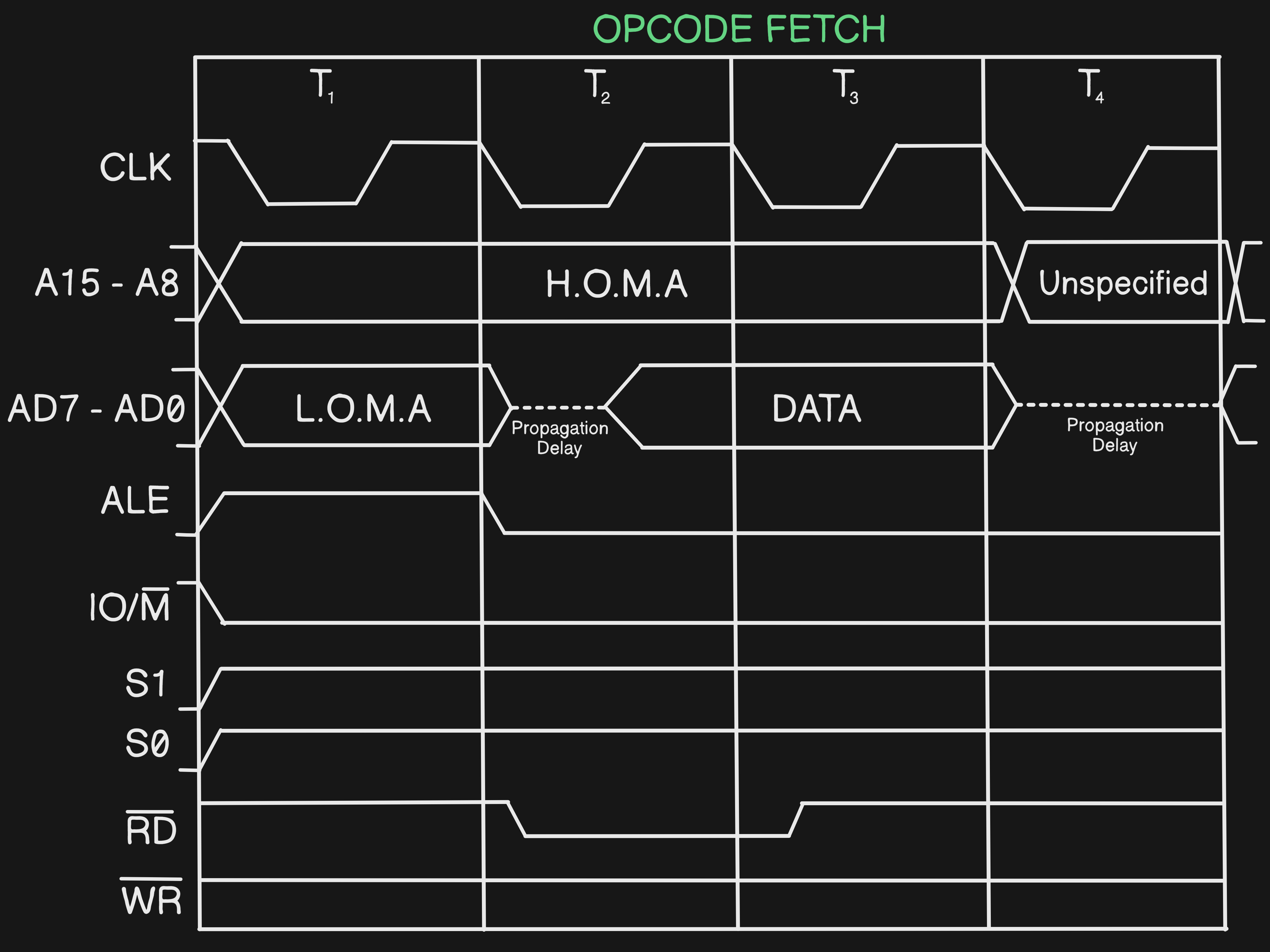
- By taking the above table as reference here is the explanation of the Opcode Fetch timing Diagram
- The First CLK is known as clock pulses, which shows the lows and the highs in the Timing Diagram and this is divided into multiple T States here in the diagram as
T1,T2,T3,T4, By using this we recognize theTransition statesin the timing diagram, and in diagram they are in50% Duty Cycleit means it’s half time low and half time high in the givenT State - ALE is
Address Latch Enablewhich facilities the data passing for more context see this question Latch Diagram - The A15 - A8 is the address which stores
H.O.M.A (Higher Order Memory Address), it means it storesHigher Nibbleand the AD7 - AD0 stores theL.O.M.A (Lower Order Memory Address), it means it storesLower Nibble. This two will complete inT3(at it only takes3T States) and the Unspecified Section is the time whereDecodinghappens. The Dotted Lines isPropagation Delay, it represents the delay time between reading and data coming into Microprocessor - IO/M (bar) will be
0as Opcode Fetch is anReading OperationandMhas bar - Both S0 and S1 will be
1 - In Opcode Fetch the RD(bar) will be
1when it’s there isno address(After L.O.M.A) in the bus as at a time there will be only one address in the bus - WR(bar), It is not used. It is high as it’s Write
Barnot Write
Q Draw the Timing diagram of Opcode Fetch and assume opcode value is47Hand store at location5000
A Just fill the data in above diagram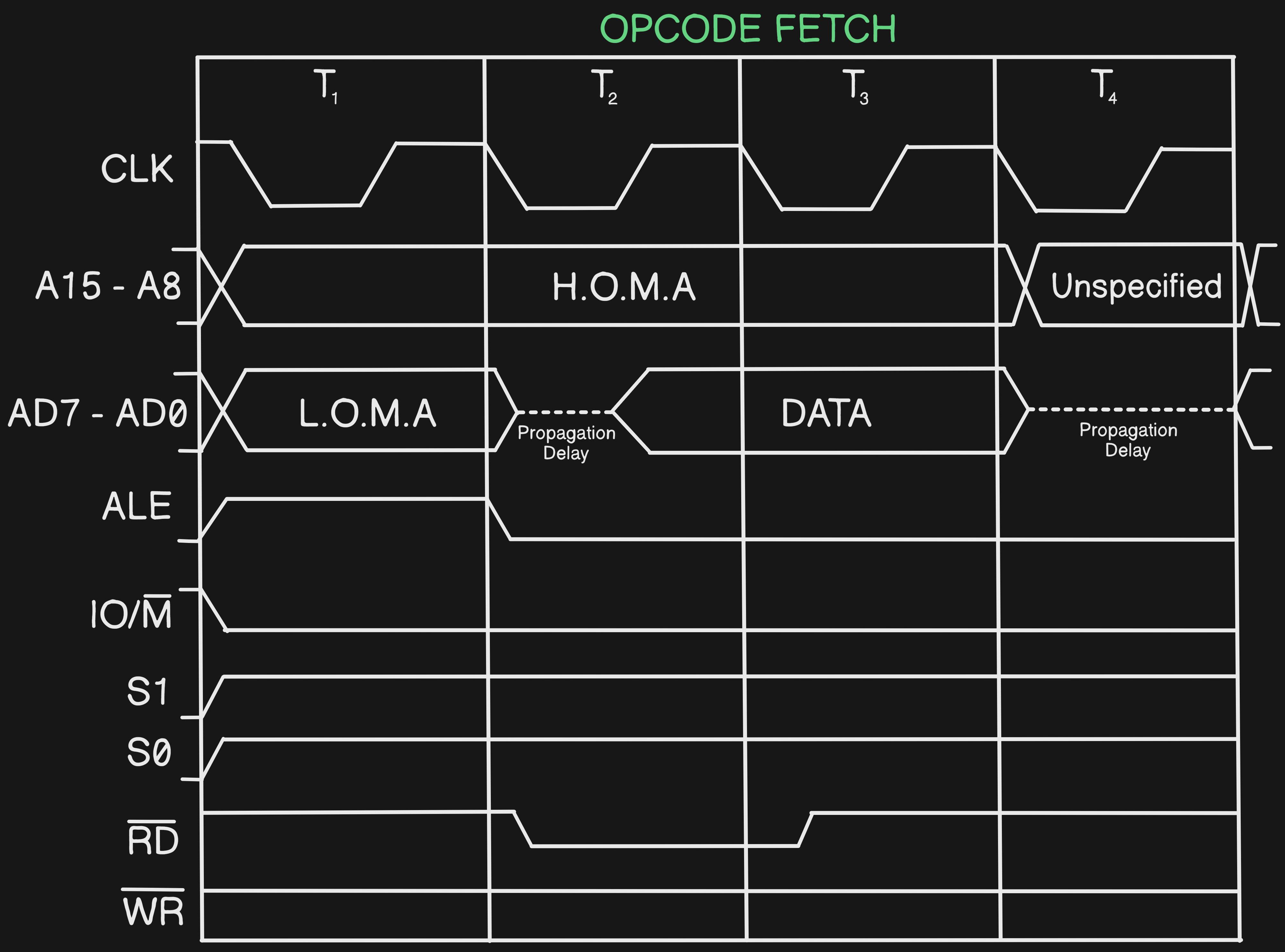 #Q Draw the Timing Diagram of
 Memory Read
A Here there will be only3TStates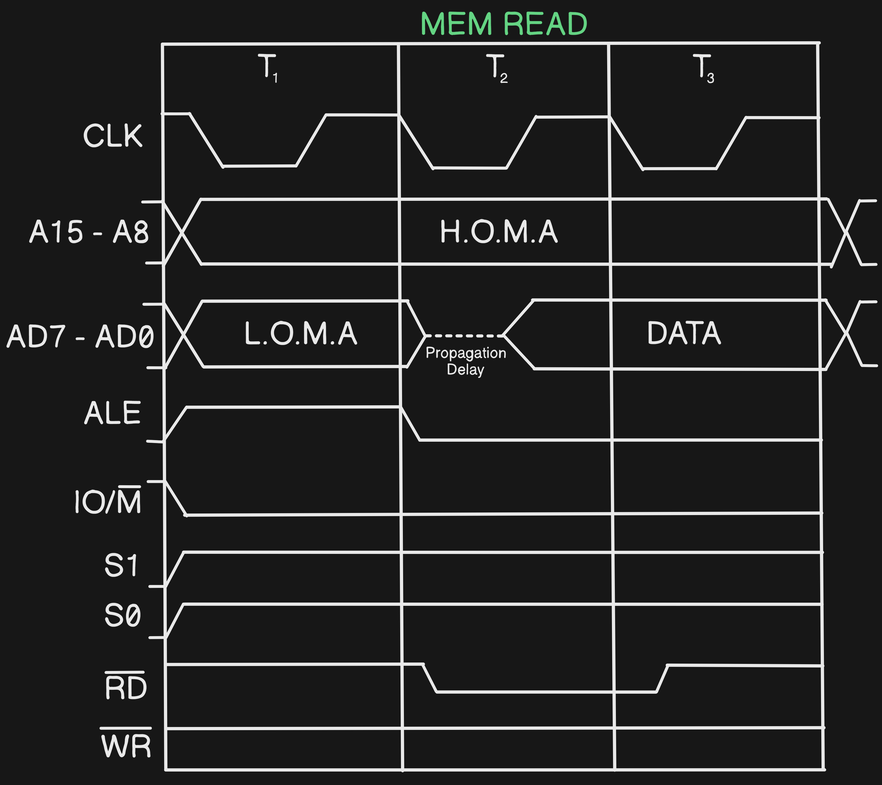 #Q Draw the Timing Diagram of
 Memory Write
A Here there will be only3TStates, And there is no Propagation Delay as it’s anWrite OperationandRD(bar)will be0andWR(bar)is1at a specific time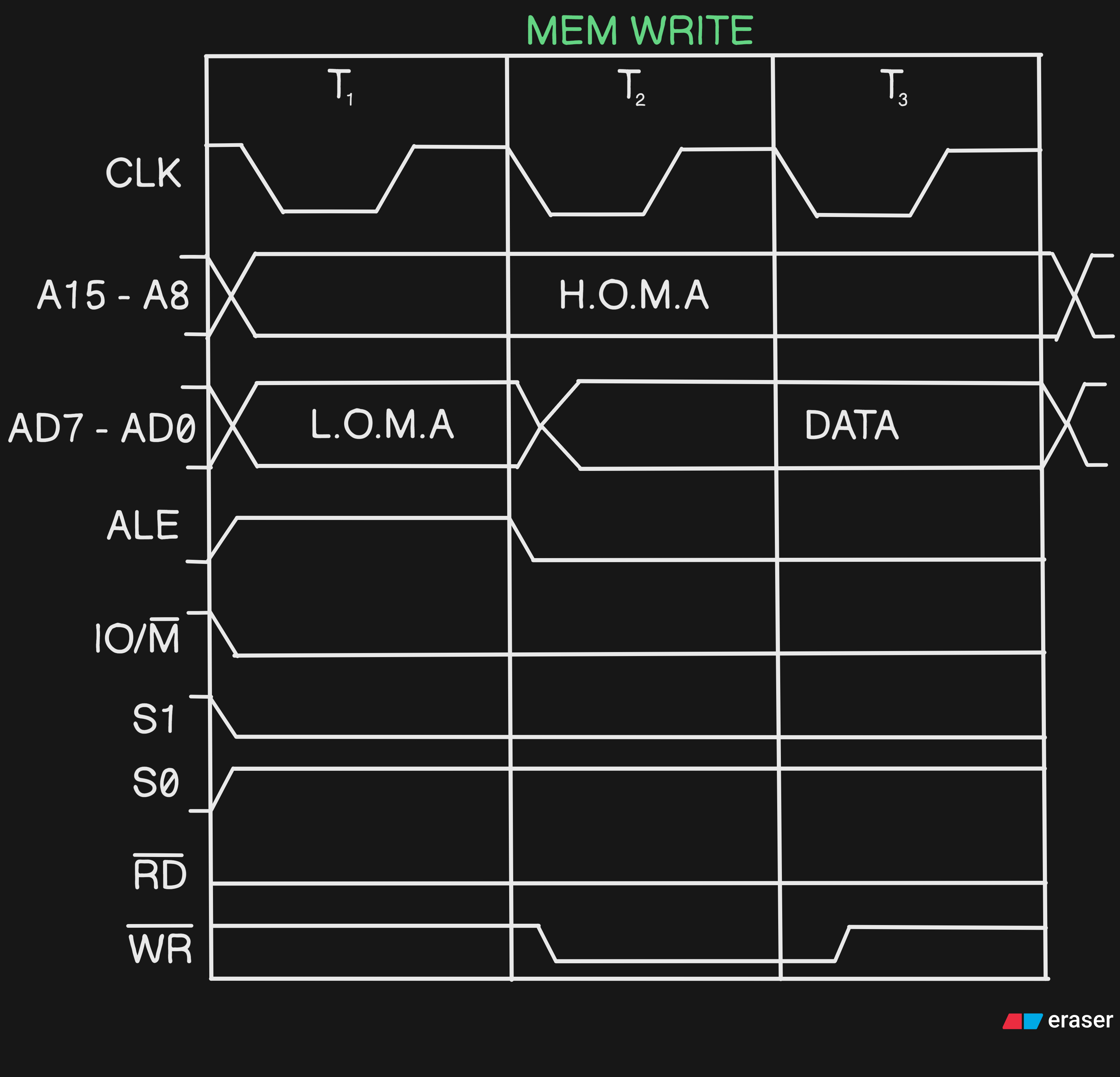 #Q Draw the Timing Diagram of
 IO Read
A In this theIO/M (bar)will be high and the data in it is 8-bit not 16-bit unlike others, here we will store the 8-bit in bothA15 - A8andAD7 - AD0(Storing same data in both the places)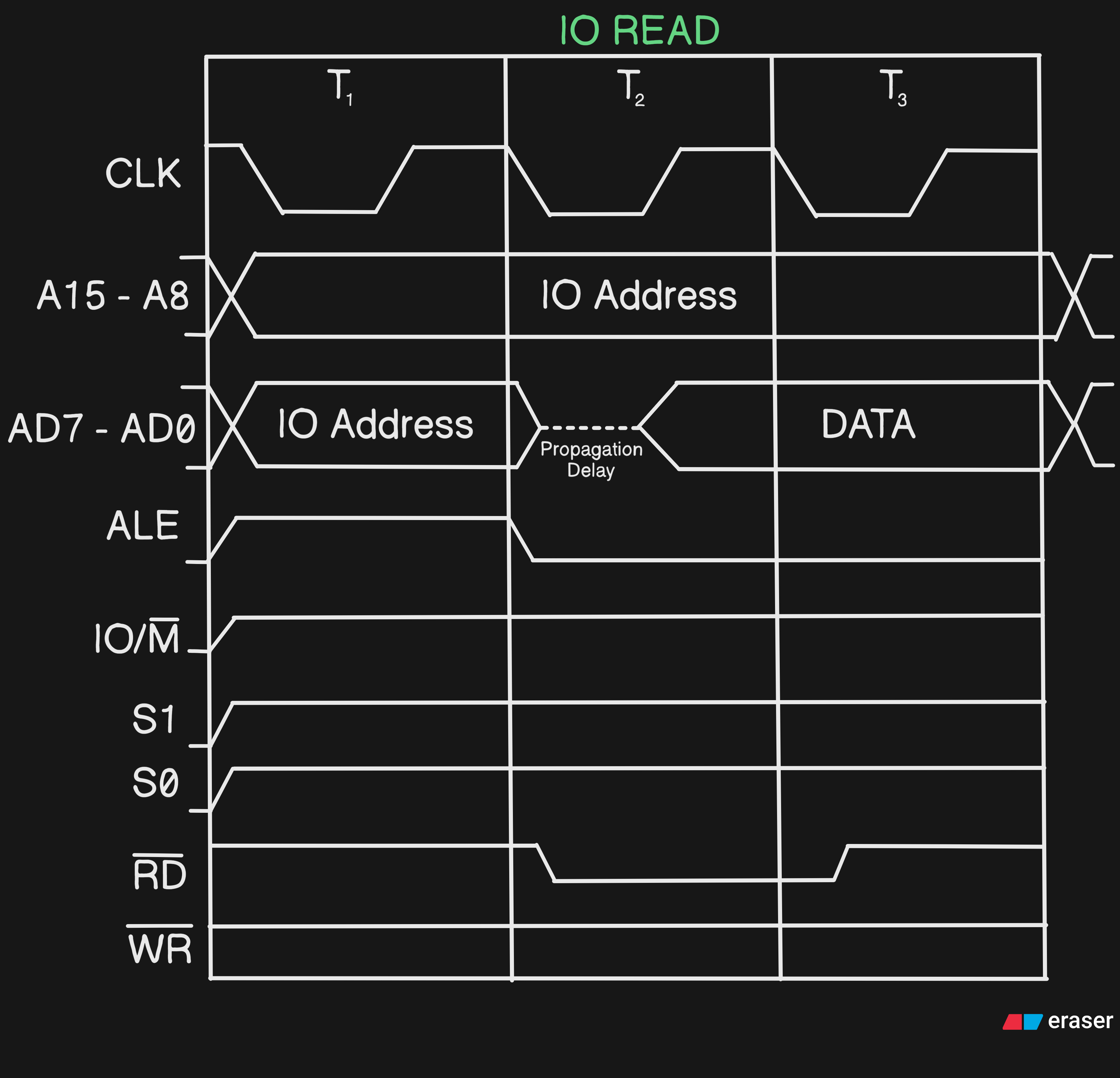 #Q Draw the Timing Diagram of
 IO Write
A In this theIO/M (bar)will be high and the data in it is 8-bit not 16-bit unlike others, here we will store the 8-bit in bothA15 - A8andAD7 - AD0(Storing same data in both the places)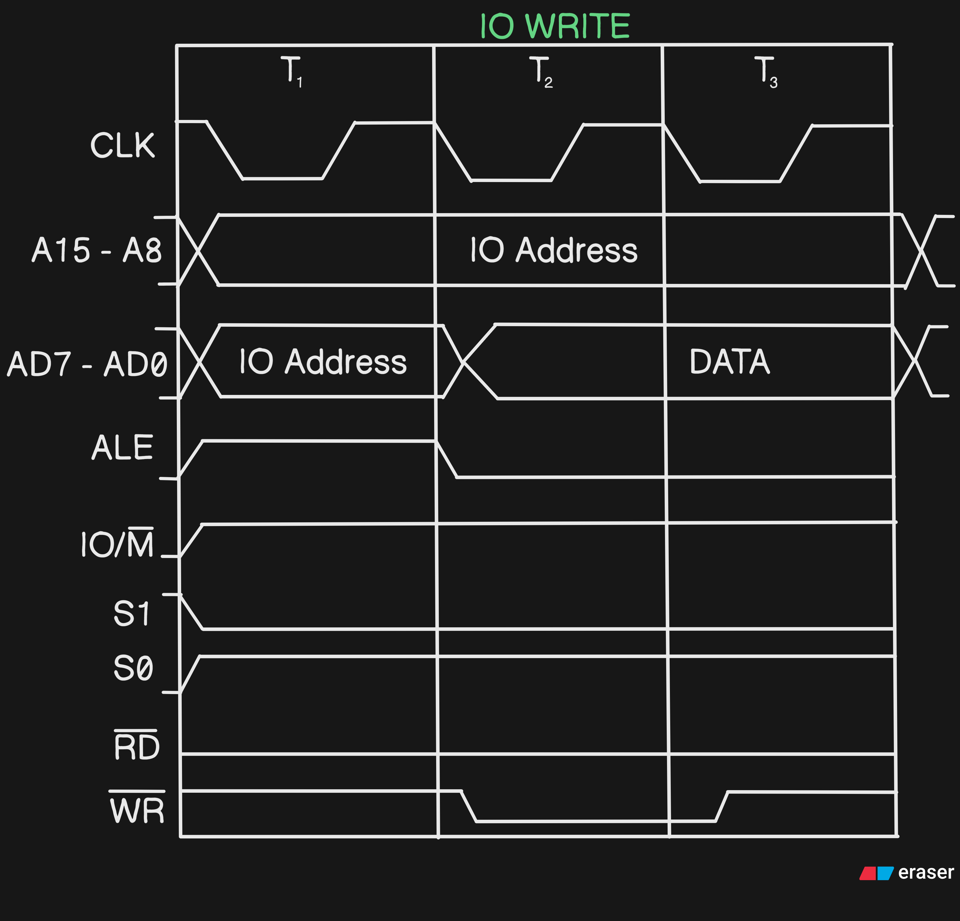 #Q Draw the Timing Diagram of
 CALLInstruction
A In this we performOpcode Fetchof6TStates, two MemoryReadsof each3TStates, two MemoryWritesof each3TStates. Let us take the data coming from3Eaddress and the data is2000H